Multilayer printed circuit boards (PCBs) have revolutionized electronic design by offering increased functionality, compactness, and enhanced performance. As technology continues to evolve, multilayer PCBs play a crucial role in powering everything from consumer electronics to aerospace applications. This article explores their structure, advantages, and key applications.Get more news about Multilayer PCB,you can vist our website!
What Are Multilayer PCBs?
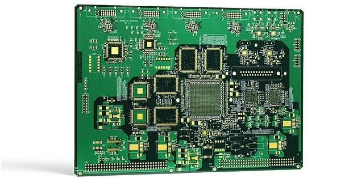
A multilayer PCB is a printed circuit board with three or more layers of conductive material separated by insulating substrates. Unlike single-layer or double-layer PCBs, multilayer designs allow for higher circuit density while maintaining a compact footprint. They are created by laminating multiple layers together, ensuring electrical connectivity between them through vias.
Advantages of Multilayer PCBs
Multilayer PCBs offer numerous benefits that make them a preferred choice in high-performance applications:
Compact Design: By stacking multiple layers, designers can reduce the overall size of the circuit while maintaining complex functionality.
Improved Electrical Performance: The layered structure minimizes electromagnetic interference (EMI) and improves signal integrity.
High Durability: Multilayer PCBs are more resistant to environmental stress, making them suitable for industrial and military applications.
Enhanced Heat Dissipation: Proper thermal management is crucial for electronic devices, and multilayer designs help distribute heat more efficiently.
Greater Flexibility in Design: Engineers have more freedom to optimize circuit layout, allowing for advanced and sophisticated electronic functions.
Applications of Multilayer PCBs
Due to their superior performance, multilayer PCBs are widely used in various industries:
Consumer Electronics: Smartphones, laptops, and gaming consoles rely on multilayer PCBs for their compact and efficient designs.
Medical Equipment: Devices like MRI machines and pacemakers use multilayer PCBs to ensure reliability and precision.
Automotive Industry: Modern vehicles incorporate multilayer PCBs for advanced control systems, infotainment, and sensors.
Telecommunications: Network infrastructure, satellites, and 5G technology depend on multilayer PCBs for stable signal transmission.
Aerospace and Defense: Military-grade electronics require robust PCBs with high durability and resistance to extreme conditions.
Challenges in Manufacturing and Design
Despite their advantages, multilayer PCBs pose challenges in manufacturing and design:
Higher Production Costs: Due to the complexity of fabrication, multilayer PCBs are more expensive than single or double-layer designs.
Difficult Repair and Maintenance: Troubleshooting multilayer PCBs is challenging due to their compact structure and internal layers.
Longer Production Time: The lamination process and additional design considerations require extra time compared to simpler PCB models.
The Future of Multilayer PCBs
With the continuous evolution of electronics, multilayer PCBs will remain a cornerstone of technological advancements. Researchers are exploring new materials and fabrication techniques to further enhance their efficiency and reduce costs. As industries demand higher performance and miniaturization, multilayer PCB technology will continue to innovate and shape the future of electronics.
By understanding the benefits and challenges of multilayer PCBs, engineers and manufacturers can optimize their designs to meet the ever-growing demands of modern technology. Whether in consumer electronics, healthcare, or aerospace, multilayer PCBs are a driving force in innovation.