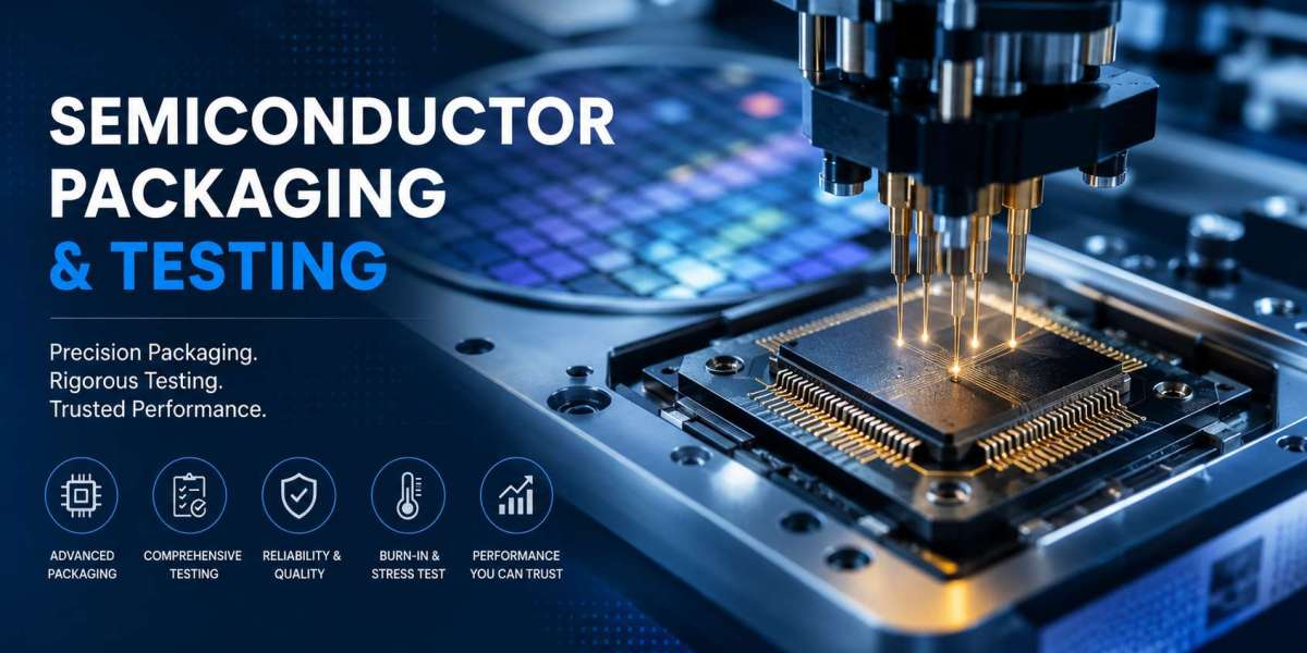

Semiconductors are at the heart of today's digital economy, powering everything from smartphones and cloud computing to autonomous vehicles and artificial intelligence. While chip fabrication is a major part of semiconductor manufacturing, the journey isn't complete until the chip has been packaged and tested. These final steps determine whether a semiconductor device is ready to perform reliably in real-world applications.
As electronic products become more compact and powerful, semiconductor packaging and testing have evolved into essential technologies that improve performance, durability, and product quality.
Understanding Semiconductor Packaging
After a silicon wafer is fabricated, it contains hundreds or even thousands of tiny semiconductor dies. Each die must be carefully separated, assembled, and enclosed in a protective package before it can be integrated into an electronic device.
Semiconductor packaging serves several important functions:
Protects the chip from environmental damage.
Creates electrical pathways between the chip and the circuit board.
Helps dissipate heat during operation.
Supports mechanical strength and long-term reliability.
Improves signal performance for high-speed applications.
Modern packaging technologies are designed to meet the growing demands of advanced electronics while reducing size and improving efficiency.
Why Testing Is a Critical Manufacturing Step
A semiconductor chip must perform flawlessly throughout its lifecycle. Even a minor defect can lead to reduced performance, system failures, or expensive product recalls. Semiconductor testing ensures that every device meets electrical, functional, and reliability requirements before shipment.
Testing helps manufacturers:
Identify defects early in production.
Increase manufacturing yield.
Verify compliance with customer specifications.
Improve overall product reliability.
Reduce operational risks in the field.
These quality checks are especially important for mission-critical industries where dependable performance is essential.
The Semiconductor Testing Process
Wafer Probe Testing
Testing begins while chips remain on the silicon wafer. Electrical probes evaluate each die to determine whether it functions correctly. Only chips that pass this stage proceed to assembly, reducing waste and improving production efficiency.
Package Assembly
Approved dies are mounted into protective packages using advanced assembly techniques. Depending on the application, manufacturers may use wire bonding, flip-chip technology, or other packaging methods to achieve the desired electrical and thermal performance.
Final Electrical Testing
Once packaging is complete, every semiconductor device undergoes final testing to verify functionality across various operating conditions. This ensures consistent quality before products leave the manufacturing facility.
Burn-In Screening
Burn-in testing exposes devices to elevated temperatures and electrical stress for an extended period. This process identifies early-life failures and increases confidence in long-term reliability.
System-Level Validation
System-Level Testing (SLT) evaluates semiconductor devices in environments that closely replicate actual operating conditions. By testing the complete device within a system, manufacturers gain greater assurance of real-world performance.
The Growing Importance of Advanced Packaging
Today's semiconductor devices support increasingly complex workloads such as AI processing, machine learning, cloud computing, and 5G communications. Traditional packaging methods are no longer sufficient for many high-performance applications.
Advanced packaging technologies provide several advantages:
Higher processing performance
Improved thermal efficiency
Greater integration density
Reduced package size
Lower power consumption
Enhanced electrical performance
These innovations enable manufacturers to deliver smaller, faster, and more energy-efficient electronic products.
Industries That Rely on Semiconductor Packaging and Testing
Virtually every technology-driven industry depends on reliable semiconductor devices. Key sectors include:
Automotive
Modern vehicles use semiconductors for advanced driver assistance systems (ADAS), battery management, infotainment, and vehicle safety. Thorough testing is essential to ensure dependable operation under demanding conditions.
Artificial Intelligence
AI accelerators and high-performance processors require advanced packaging to handle massive computational workloads while maintaining efficient thermal performance.
Data Centers and Cloud Computing
Servers and storage systems rely on reliable semiconductor components to deliver uninterrupted performance and support large-scale digital infrastructure.
Telecommunications
5G networks and communication equipment require high-speed semiconductor devices capable of maintaining signal integrity and consistent performance.
Industrial Automation
Factories, robotics, and Industrial IoT applications depend on durable semiconductor components that can operate reliably in challenging environments.
The Value of OSAT Services
Outsourced Semiconductor Assembly and Test (OSAT) providers play a vital role in the semiconductor ecosystem. By offering specialized expertise in packaging, assembly, and testing, OSAT companies help semiconductor manufacturers reduce production complexity and accelerate time to market.
Their services typically include:
Wafer probing
Semiconductor assembly
Advanced packaging
Final electrical testing
Burn-in services
System-level testing
Reliability analysis
Partnering with an experienced OSAT provider enables chip designers and manufacturers to focus on innovation while ensuring high production quality.
Looking Ahead
As semiconductor technology continues to advance, packaging and testing will become even more important. Emerging technologies such as chiplets, heterogeneous integration, and AI-driven electronics demand packaging solutions that deliver higher performance in increasingly compact designs.
At the same time, comprehensive testing will remain essential for ensuring that these advanced devices meet the strict quality and reliability standards expected across global industries.
Conclusion
Semiconductor packaging and testing are much more than the final steps of manufacturing—they are the foundation of reliable electronic products. By combining innovative packaging technologies with rigorous quality testing, manufacturers can deliver semiconductor devices that power the next generation of computing, communications, automotive systems, and artificial intelligence.
As the semiconductor industry evolves, investment in advanced packaging and testing capabilities will continue to drive innovation, improve product reliability, and support the growing demand for high-performance electronics worldwide.